PCB routing and circuit designing is not only a part of engineering, it is an art as well. With modern electronics, PCB designing has proven crucial for any electronics product to come out as functionally successful. Therefore, it is indeed important to follow PCB designing principles.
If you are a beginner in the field of electronics, it might get difficult or confusing to properly handle all the aspects of PCB designing. It goes without saying that there is a lot that goes into any design engineering and PCB design is not an exception. It could make or break any product. There are several PCB designing software that are most commonly used such as Alyuim Designer, EAGLE (Easily Applicable Graphical Layout Editor), Multism, OrCAD, KiCAD, EasyEDA. So, let’s go into detailed guidelines for beginners to start with PCB designing.
1st Step: Designing Schematics
Schematics play a key role in the PCB designing process. It is a blueprint of an electronics product. During schematics design, designer needs to cover following details:
- What kind of components will be part of your design
- How all these components are connected altogether
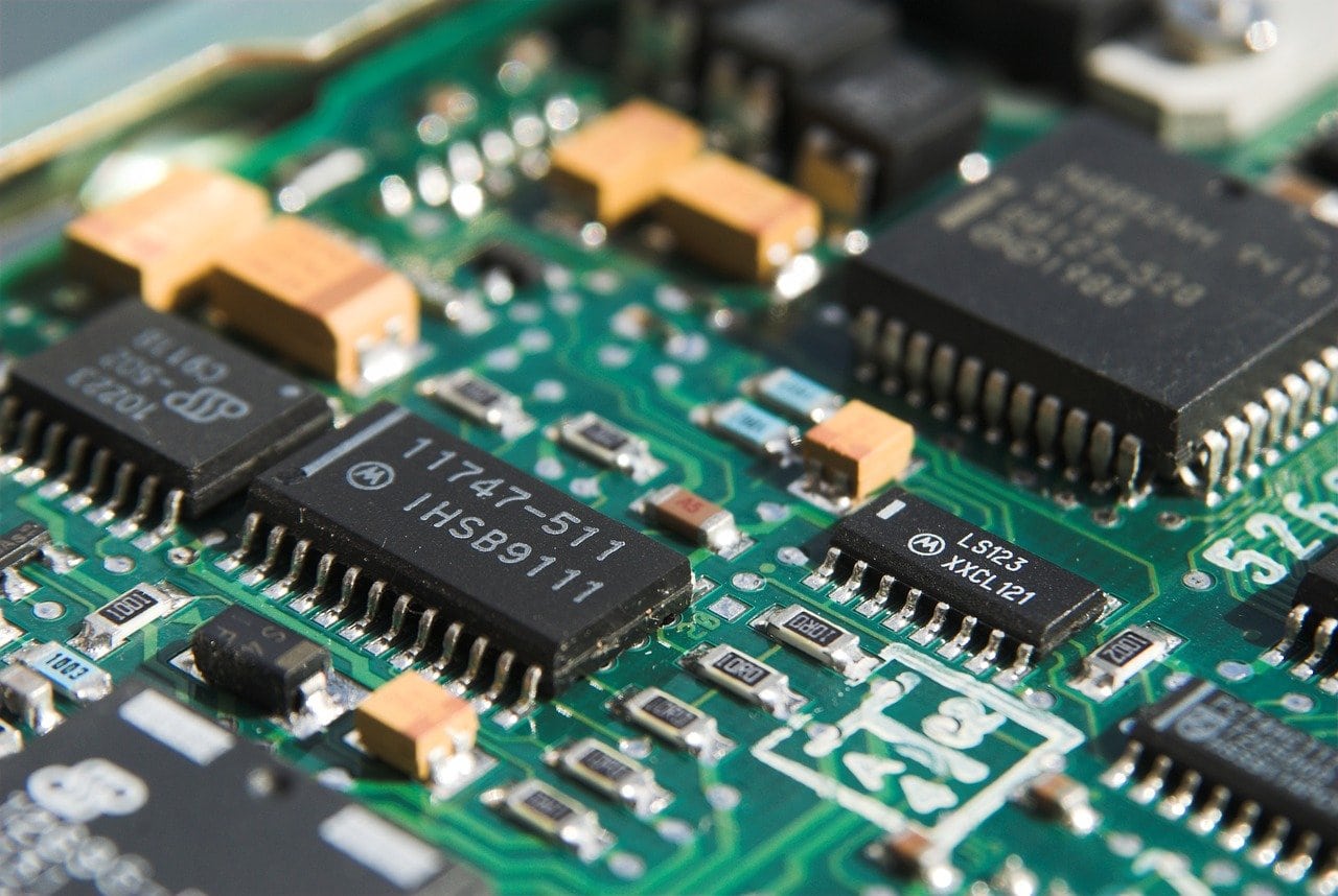
2nd Step: Designing layouts
After finishing up with schematics, you need to generate a PcbDoc file to import all components into the PCB layout. Here you need to figure out the shape and size of PCB and layer stack up.
3rd Step: Synchronizing schematics with PCB
Linking schematics with PCB can be done by following these steps in your design software; This may slightly vary as per various software:
- Go to design and update PCB
- A new dialogue box will pop up, where you need to verify all changes as you keep adding new information to PCB from schematics.
- A green tick mark or Validated sign indicates changes are valid and you can execute those changes
4th Step: Deciding on PCB layer stackup
With the help of a layer stack up manager on your chosen software, you need to define size, shape and number of layers in your PCB.
5th Step: Defining PCB design rules
It is recommended to follow globally known standards for deciding PCB design rules such as IPC standard. PCB design rules include following criterias:
- Clearance among various components, pads and traces in PCB layout.
- Routing rules accommodating trace width and length for various nets
- High speed, voltage and signal integrity limits
6th Step: Placing components
Depending upon your design software you can choose to place all components manually or automatically or mix of both.
7th Step: Include drill holes
It is advisable to insert drill holes before you begin to route traces. For that, you need to follow the design for manufacturing (DFM) specification from your PCB manufacturer.
8th Step: Routing traces
When you begin routing traces in your PCB, you should start with important routes first, such as power nets, RF (Radio Frequency) related nets, or any other impedance controlled nets or noise sensitive nets. Afterwards you can finish up with remaining connections. It is important to follow few constraints for such nets:
- Traces with low voltage nets should not be overlapped with high voltage nets from different layers.
- Noise sensitive traces should be kept as short as possible.
9th Step: Adding the labels
After completing routing it is vital to add labels, identifiers, markings, logos and other imagery to silkscreen. It is important to include Pin 1 indicators, polarity marking for bipolar components or any other labels that can be proven crucial for the assembly process or debugging the PCB afterwards. All these labels and markings are required to be placed in the Top Overlay or Bottom Overlay layers in the PCB layout.
10th Step: Generating design output files
Design files for manufacturing PCB are generated as Gerber files, IPC-2581 or ODB++, which are various standard formats for PCB.